Skip to content
KOEN

Insights

Reports, briefs and technical notes from Cools on semiconductor packaging technology and industry.

33 results

Sort: Newest
검은 배경 위에 쿨스 로고와 TECHNICAL NOTE 라벨, 흰색 큰 글씨로 SIC FOCUS RING이 적힌 썸네일.Technical noteEquipment parts

A near-net SiC core, precursor-derived SiC functional layer and HIP for semiconductor chamber parts

This Technical Note describes a manufacturing platform for semiconductor chamber parts such as focus rings and edge rings, in which a reaction-filled SiC core and a precursor-derived SiC functional layer take on separate roles. It covers the design principles, the process flow and the evaluation plan. The full report is available in Korean. An English summary is provided on this page.

검은 배경에 쿨스 로고와 TECHNICAL NOTE 표기, 가운데 EIC-PIC BONDING 문구가 놓인 테크니컬 노트 썸네일.Technical noteThermal control

Oven annealing and 1500 nm interface-selective heating

In a COUPE structure, the heat is needed at the bonding interface between the EIC and the PIC. Oven annealing instead puts heat into the entire assembly, including the support silicon and the optical devices. This technical note sets out what that difference changes in a structure whose optical paths and coupling alignment are sensitive to heat. The full report is available in Korean. An English summary is provided on this page.
검은 배경에 쿨스 로고와 TECHNICAL NOTE 라벨, 가운데 HBM 12-HIGH 문구가 흰색으로 들어간 이미지.Technical noteHBM

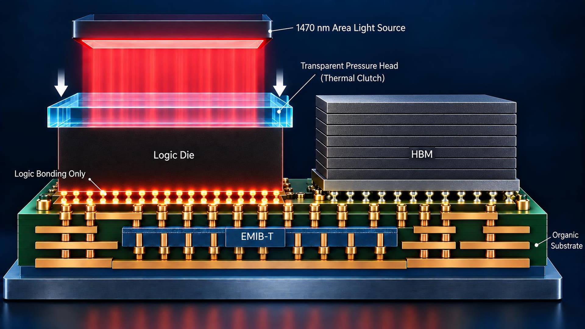
Cools completes a 12-high HBM stack with dielectric-first bonding and a single-shot copper join

As HBM stacks reach 12 layers, the dies get thinner and the number of interfaces grows. Bonding and annealing layer by layer, or stacking the dielectric first and annealing the whole assembly in an oven, both put the entire stack through a thermal history. This technical note describes a process that fixes all 12 layers by dielectric bonding first and completes the copper joins in a single 1500 nm photothermal exposure. The full report is available in Korean. An English summary is provided on this page.