Technical noteGlass substrates
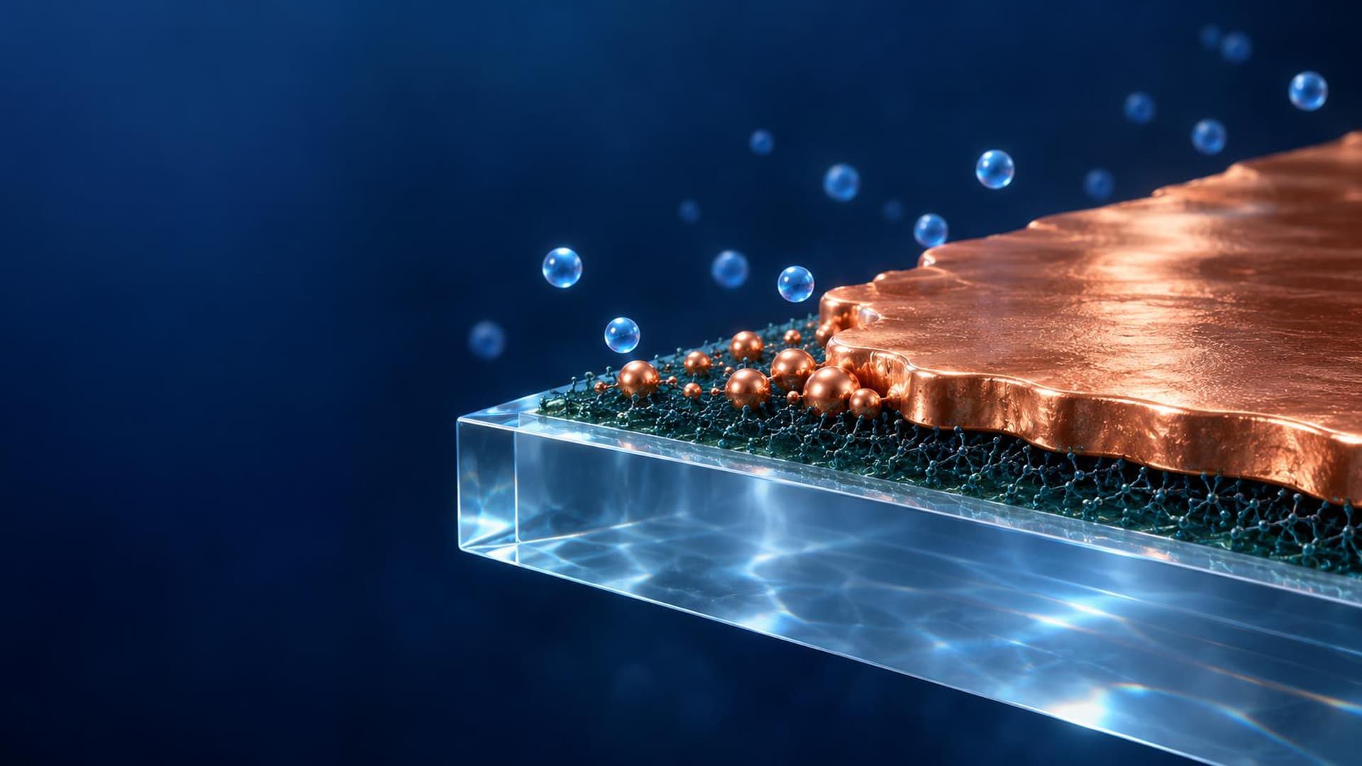
Full-length PDA bonding that closes the central adhesion gap for long-term glass via reliability
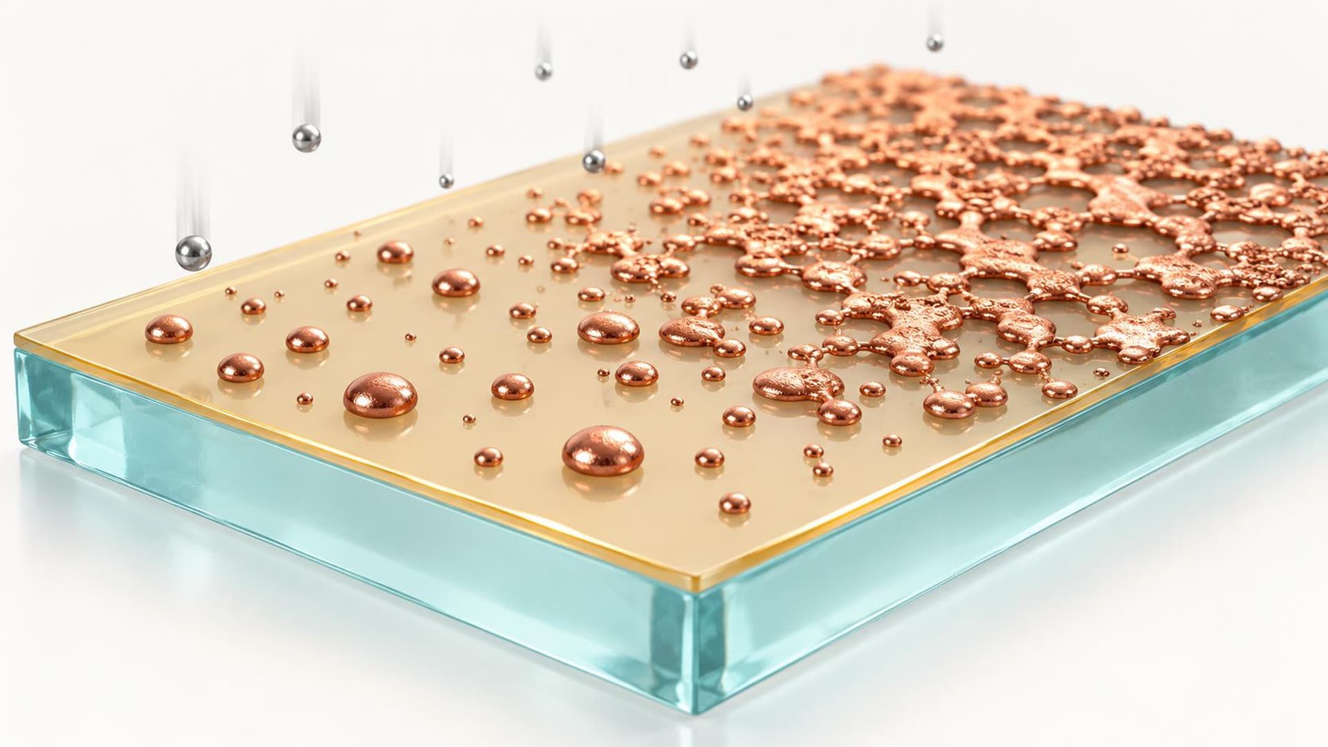
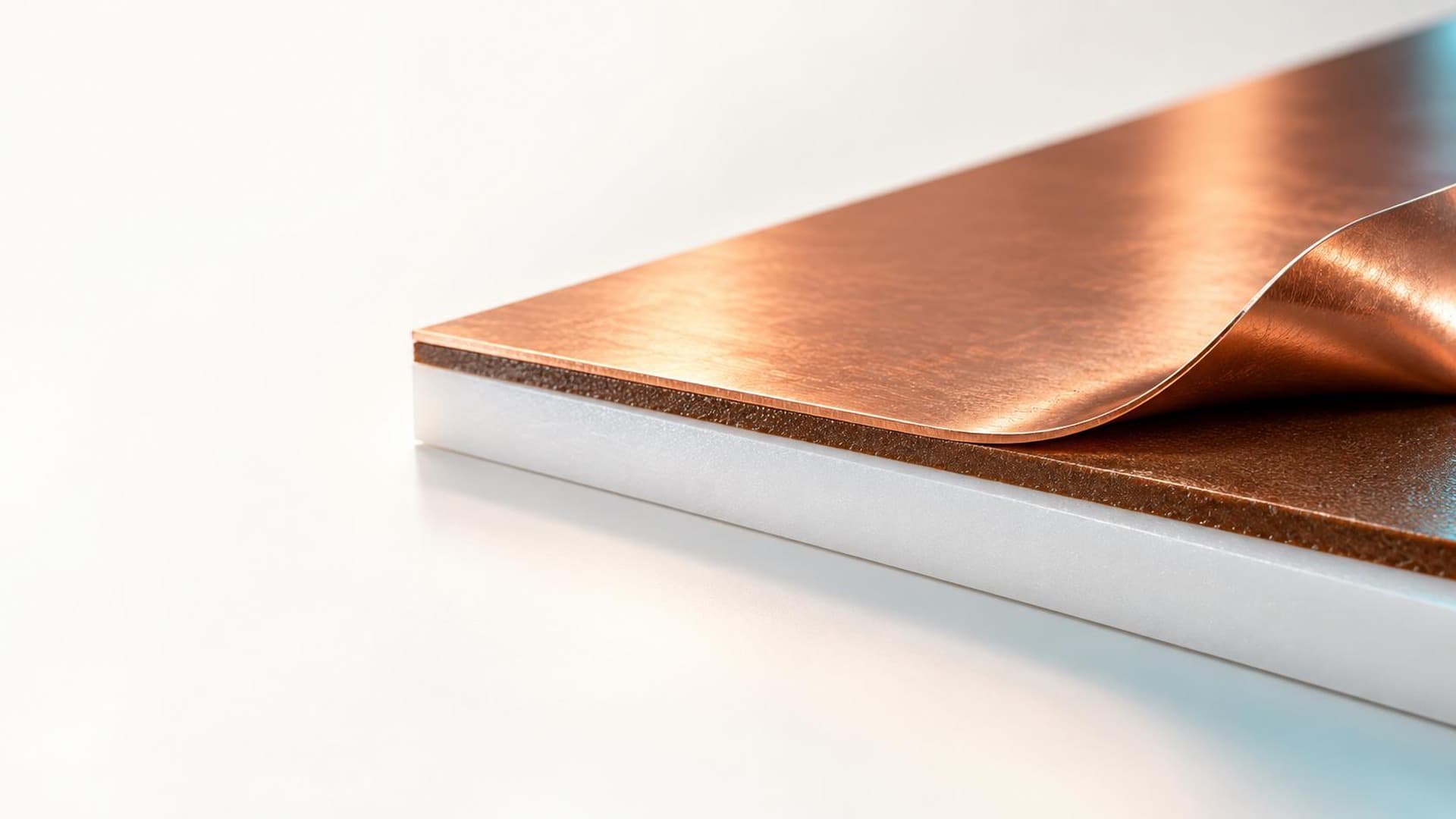
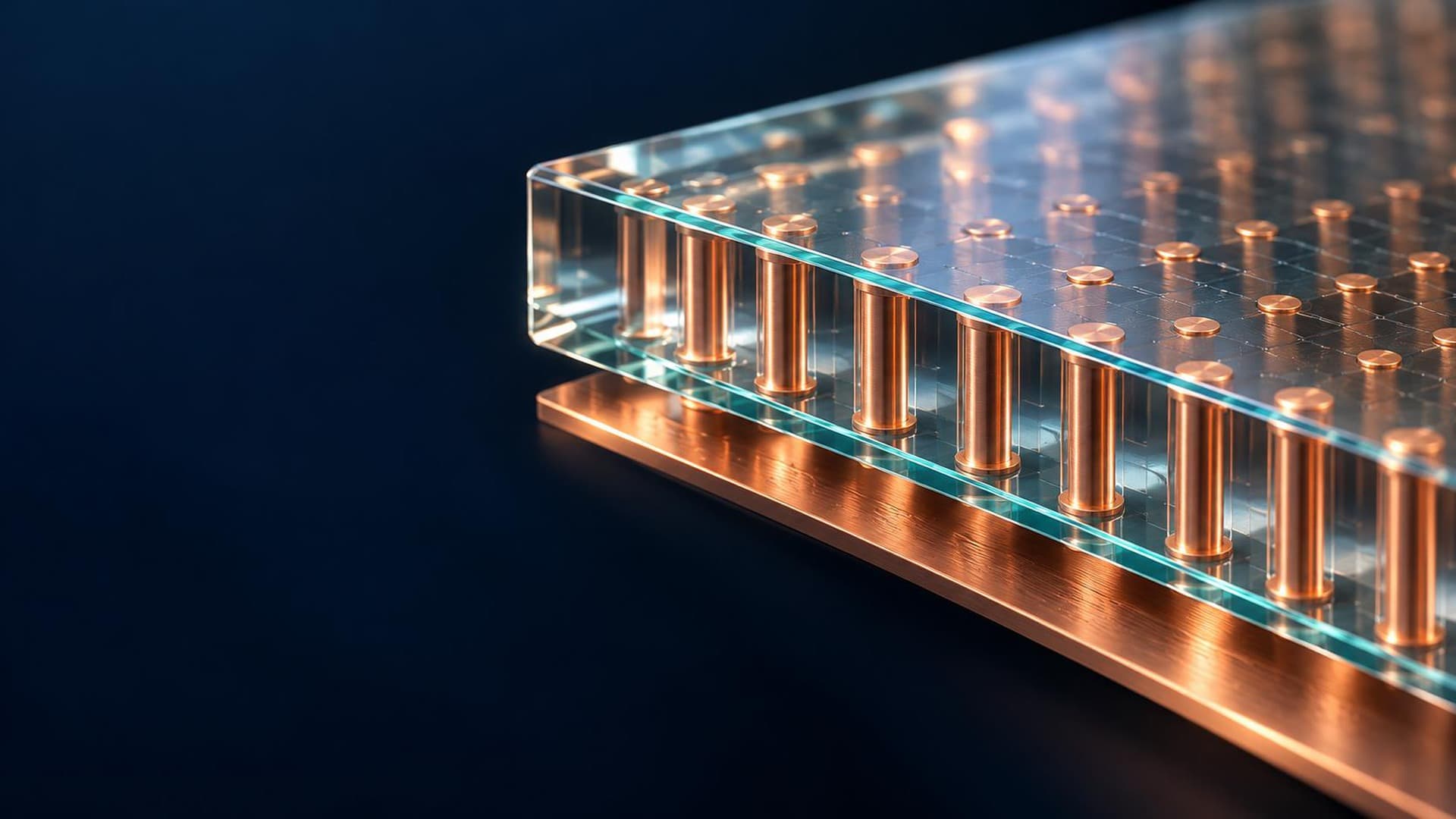
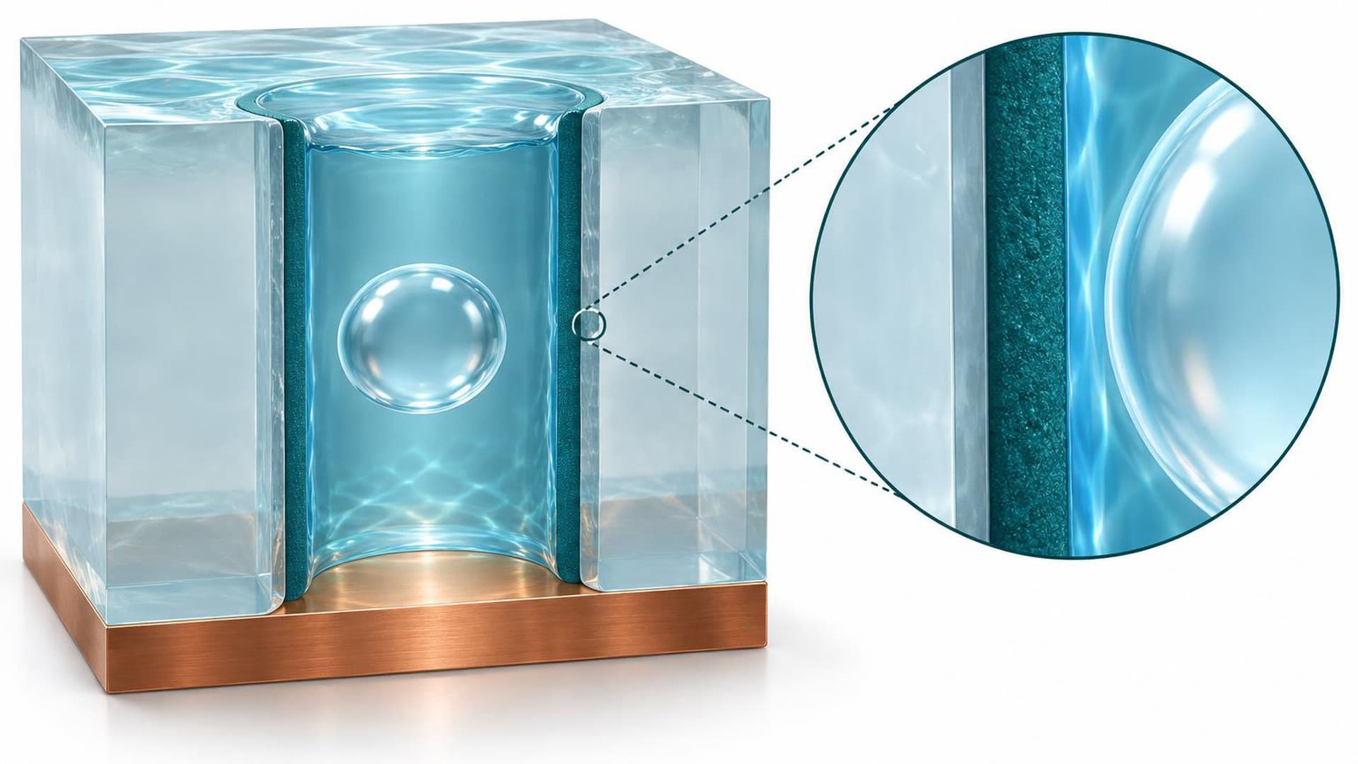
Glass vias metallized by double-sided sputtering bond only at the entry and exit, leaving an adhesion gap in the middle. This Technical Note uses a Corning patent and thermal cycling literature to examine how that gap becomes a damage path under repeated thermal deformation, and compares it with a PDA full-length bonding structure that extends the bond to the via center.