About this document
This Technical Note addresses the two places where heat becomes a problem in co-packaged optics: the EIC–PIC bonding process and the thermo-optic tuners inside the PIC. It describes how the heat path is designed for each location. The full report is available in Korean. An English summary is provided on this page.
Download
An English edition is not available yet. The Korean document is below.
Summary
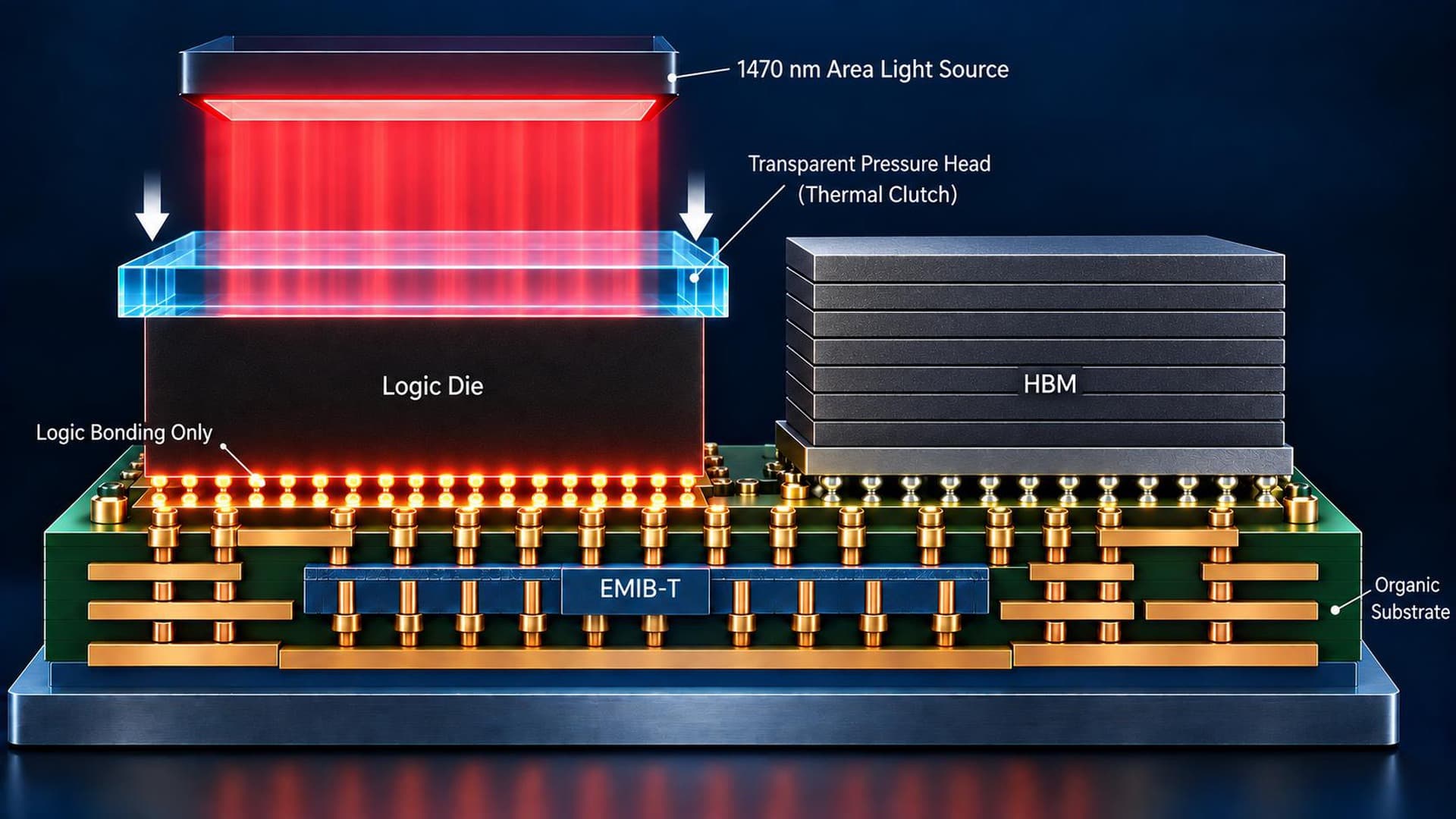
In CPO bonding, the heat needed at the joints spreads to nearby optical devices, and inside the PIC a thermo-optic tuner either responds slowly when insulated or draws high holding power when heat-sunk. An Optical Thermal Clutch that heats only the joints with 1,500 nm light, and a Micro Thermal Clutch that separates a thermal delay layer from a heat-spreading layer under the heater, address the two problems.
Conclusion
Heat causes trouble in CPO at two points. One is the bonding of the EIC to the PIC: conductive TCB heating or whole-oven heating carries the heat needed at the joints into the surrounding PIC. The other is the thermo-optic tuner inside the PIC. Insulating the heater saves power but slows switching and recovery of optical modulation; bonding it directly to silicon speeds the response but raises holding power. Cools treats both as a question of designing the heat path to match where and when heat is needed. At the joints, Cools uses the Optical Thermal Clutch. Nanosecond pulses of 1,500 nm light, below the silicon bandgap, pass through silicon and are absorbed in a Ti-based layer behind each pad. Heating is concentrated in the pad and absorber, and once the pulse ends the heat spreads into the surrounding silicon substrate, which cools the joint on its own. Inside the PIC, Cools uses the Micro Thermal Clutch. In a single thermal resistance–capacitance approximation, holding power scales inversely with thermal resistance (Phold ≈ ΔT / Rth) and response time with the product of thermal resistance and effective heat capacity (τ ≈ Rth · Ceff). Raising thermal resistance alone slows the response, so the design splits the roles: a low-conductivity delay layer directly under the heater provides the resistance that cuts holding power, a small heated region lowers the effective heat capacity to speed the response, and a high-conductivity spreading layer prevents heat build-up underneath for stable repeated operation. The document states that the Micro Thermal Clutch performance shown in its three-structure comparison is a Cools design target. The approach extends to the thermo-optic bias and phase tuners of thin-film lithium niobate (TFLN) devices, where the Pockels effect handles high-speed modulation and heat sets the operating point and phase. Used together, the two technologies address PIC heat exposure and package deformation during bonding, tuning power and settling time in operation, and thermal crosstalk as channel counts grow, within one thermal design.
Topics
- CPO
- Thermal control