Skip to content
KOEN

Insights

Reports, briefs and technical notes from Cools on semiconductor packaging technology and industry.

8 results

Sort: Newest
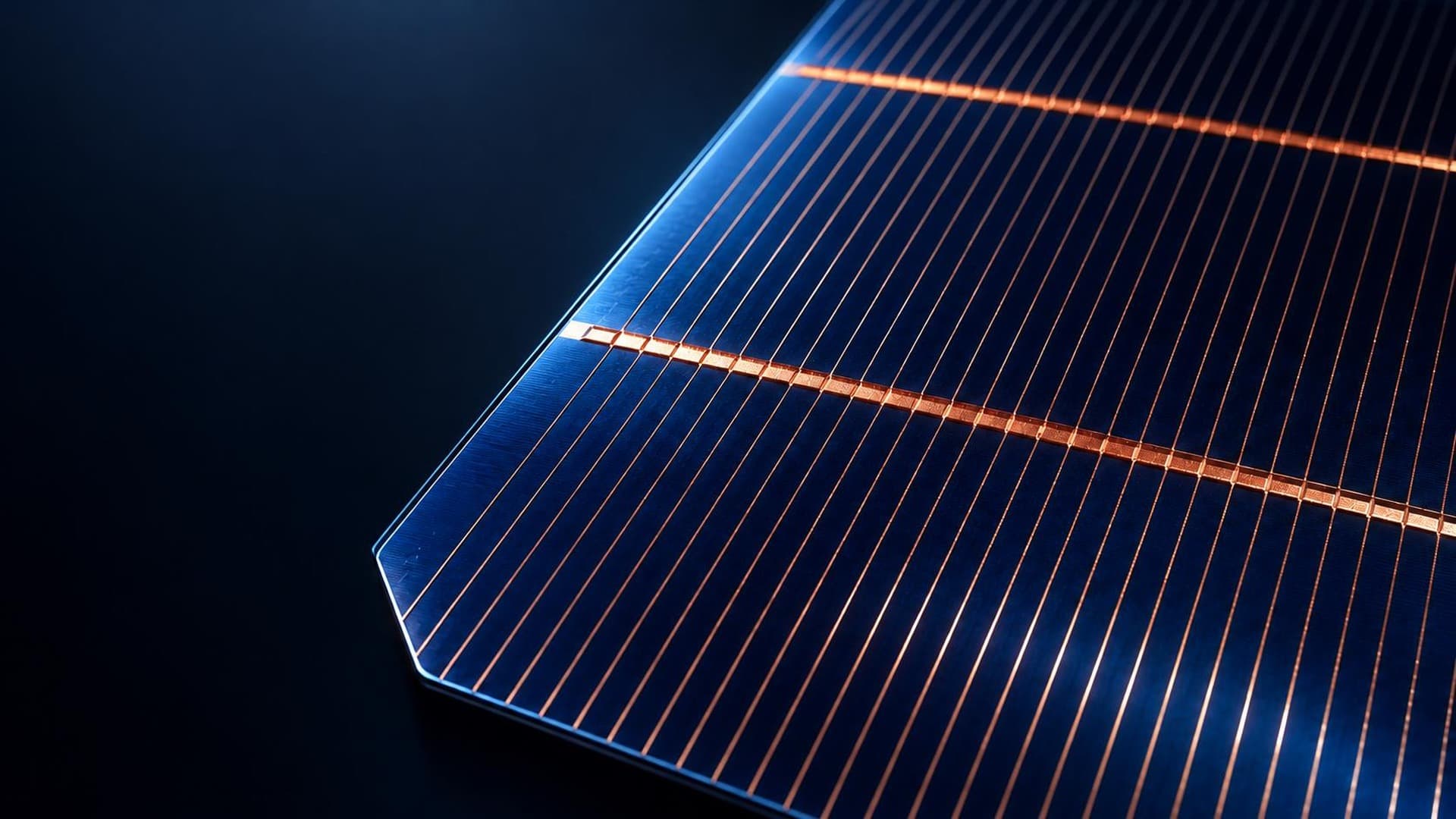
햇빛이 반사되는 태양광 모듈 여러 장을 비스듬히 내려다본 사진. 파란 셀 격자 위로 오른쪽 위에서 주황빛 햇빛이 번진다.BriefSolar

A dual-wavelength perovskite process that uses coordination state as a manufacturing variable

This brief treats two problems usually handled separately in solution-processed perovskite films, residual DMSO removal and defect sealing, as one manufacturing variable: coordination state. It outlines a process that controls both with two wavelengths applied in sequence, together with a validation design. The full report is available in Korean. An English summary is provided on this page.

검은 배경에 쿨스 로고와 TECHNICAL NOTE 라벨, 흰색 대형 글자로 RBSC PLATFORM이 적힌 테크니컬 노트 썸네일.Technical notePower semiconductors

Ultrathin InP and Ga₂O₃ layers on an RBSC platform for photonic and power semiconductors

InP and Ga₂O₃ share two constraints: low thermal conductivity and costly single-crystal substrates. This Technical Note describes a common manufacturing platform that transfers only the functional layer onto a reaction-bonded silicon carbide (RBSC) support and joins it by interface-selective optical heating. The full report is available in Korean. An English summary is provided on this page.

검은 배경에 쿨스 로고와 TECHNICAL NOTE 라벨, 흰색 대형 글자로 PHOTONIC BONDING이 적힌 테크니컬 노트 썸네일.Technical notePhotonics

Interface-selective bonding for heterogeneous integration in silicon photonics

In heterogeneous silicon photonics integration, each added material exposes heat-sensitive optical devices to the bonding temperature again. This Technical Note sets out the principle, process and equipment of interface-selective bonding, which converts light into heat only at the designed bond interface. The full report is available in Korean. An English summary is provided on this page.

검은 배경 위에 쿨스 로고와 TECHNICAL NOTE 라벨, 흰색 큰 글씨로 III-V PV GLASS가 적힌 썸네일.Technical noteSolar

Single-crystal III–V power-generating glass with transmittance and output set by layer thickness

Semi-transparent solar cells divide a single absorber between daylighting and power generation. This Technical Note describes a manufacturing approach in which the thickness of a single-crystal III–V layer, set by the exfoliation depth, fixes both transmittance and output as product specifications. The full report is available in Korean. An English summary is provided on this page.