About this document
In a COUPE structure, the heat is needed at the bonding interface between the EIC and the PIC. Oven annealing instead puts heat into the entire assembly, including the support silicon and the optical devices. This technical note sets out what that difference changes in a structure whose optical paths and coupling alignment are sensitive to heat. The full report is available in Korean. An English summary is provided on this page.
Download
An English edition is not available yet. The Korean document is below.
Summary
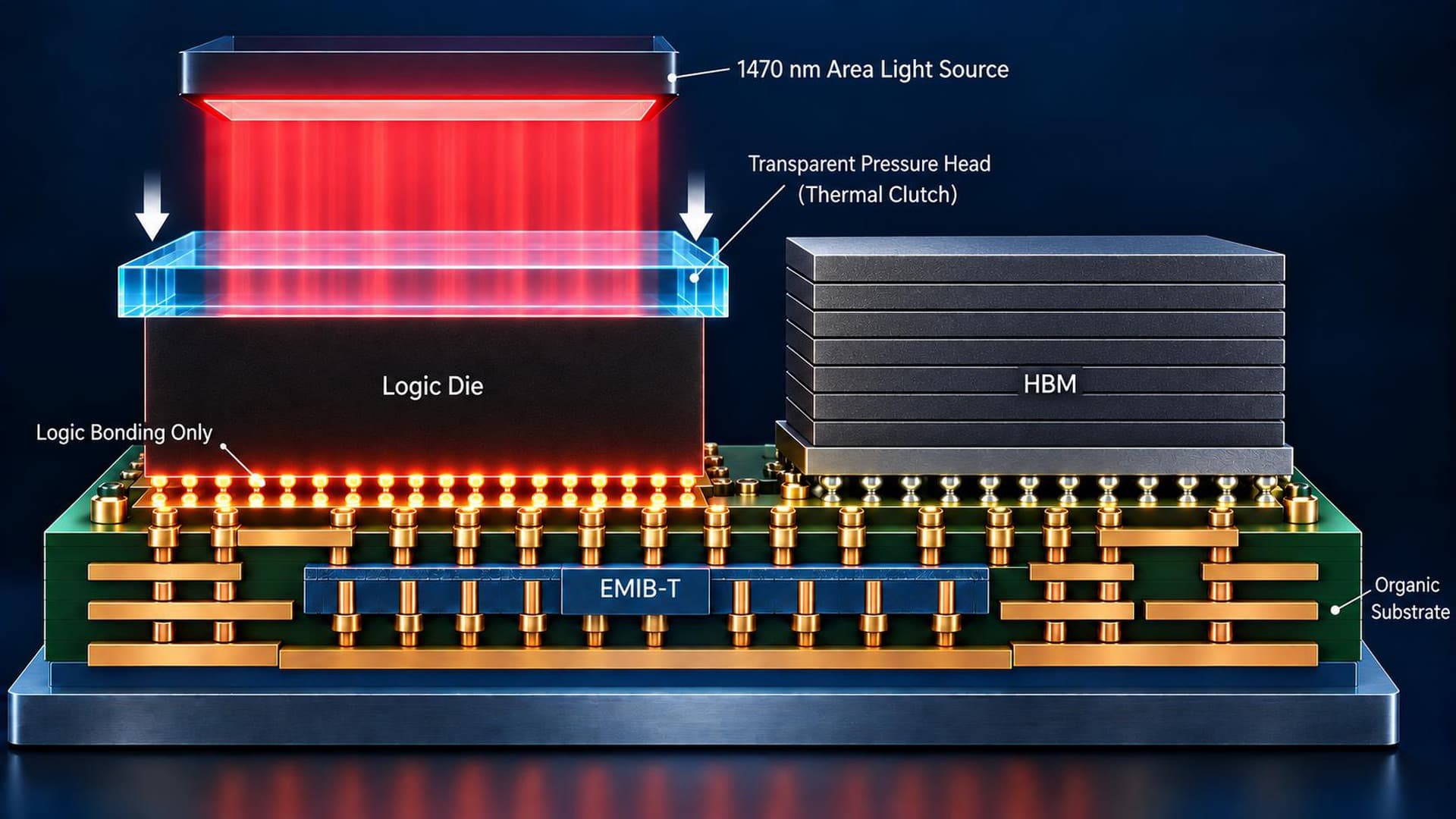
Completing the Cu bonding of hybrid bonding requires heat, but the location where it is required is the EIC-PIC bonding interface. Oven annealing applies a heating ramp, a hold, and cooling to the entire stack, so the optical structures and coupling alignment of the PIC also undergo a thermal history. Light at 1500 nm passes through silicon and is converted into heat only in the absorbing layer on the back side of the pad. The irradiation is applied broadly with a surface light source, but heat is generated only at the bonding region, so multiple pads within the irradiated area are processed at once while the thermal burden on the PIC is kept low. This piece addresses the structure that limits both the heating location and the duration, and the process transition path for it.
Notes from validating a drop-in cooling module on existing bonders: what was measured, under which conditions.
Conclusion
Heat is needed at the bonding interface and must be kept out of everything around it. Oven annealing cannot separate the two requirements. Heat supplied from outside flows into the EIC, the PIC and the support structure alike, and the PIC takes on thermal deformation, alignment shift and thermal load on its optical devices together. Optical coupling is managed to submicron reference positions, so these effects show up directly as performance. A 1500 nm planar source illuminates broadly but heats selectively. The silicon substrate on the incident side serves as the transmission path, and the absorber behind each pad converts the optical energy into heat. With the copper recess still present, instantaneous thermal expansion makes contact and repeated pulses form the bond. For the same bonding interface, the difference is not temperature but its distribution in space and time. In the conventional route the whole assembly is hot for the full oven hold; with selective heating the interface is hot only during the pulse exposure. Because the planar source heats every pad within the illuminated field at once, large-area batch processing and interface-selective heating hold at the same time. The silicon and the PIC between the dies and pads outside that field do not act as heat sources. The result is a process that completes the copper joins while suppressing thermal deformation of the PIC and protecting its alignment and optical characteristics.
Topics
- Thermal control
- CPO