About this document
For electroless copper on metal-oxide adhesion layers used in through-glass via metallization, this Technical Note reviews papers and patents on the internal defects of the copper seed and the effects of heat treatment, which must be checked separately from adhesion to glass.
Download
An English edition is not available yet. The Korean document is below.
Summary
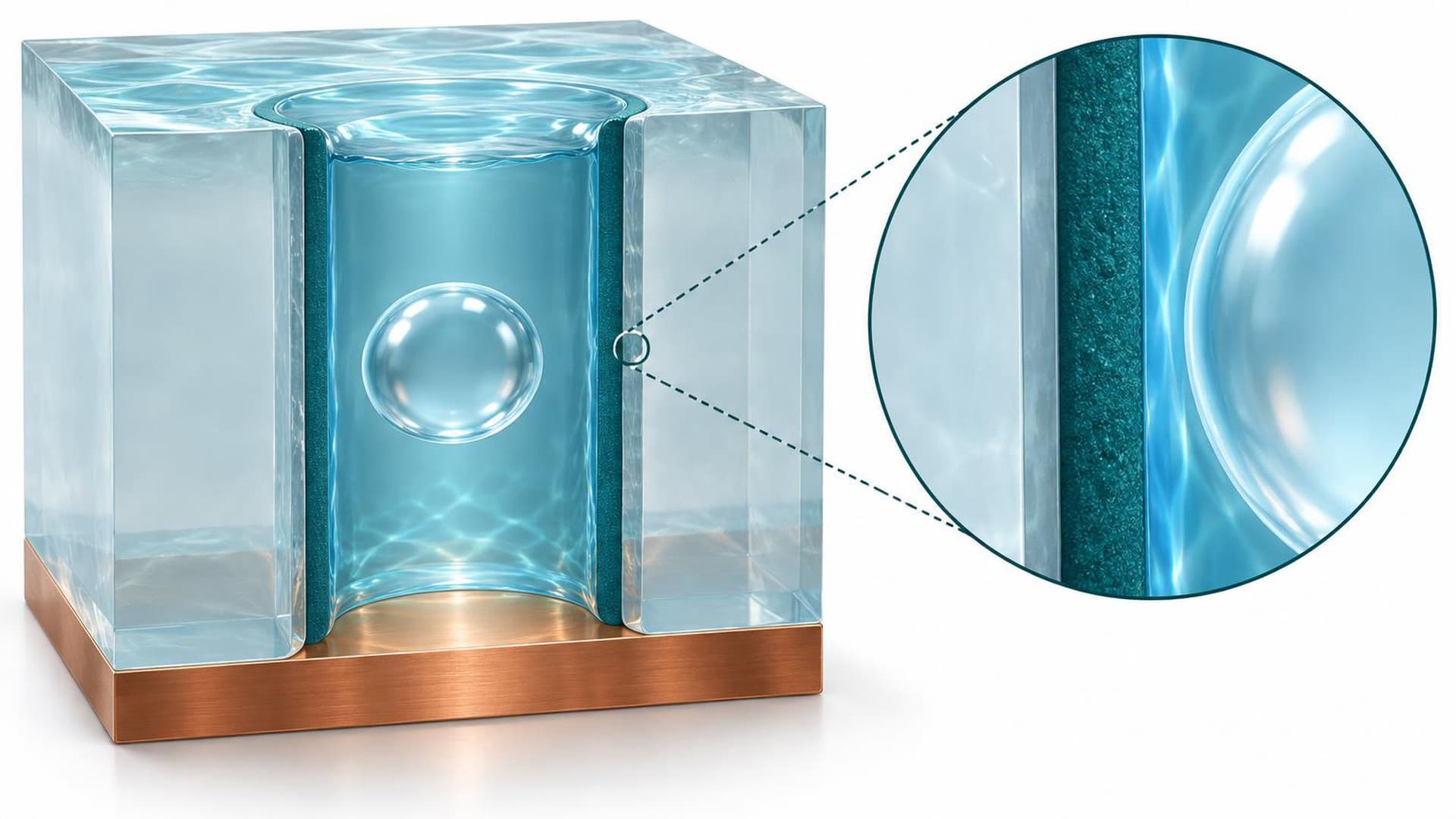
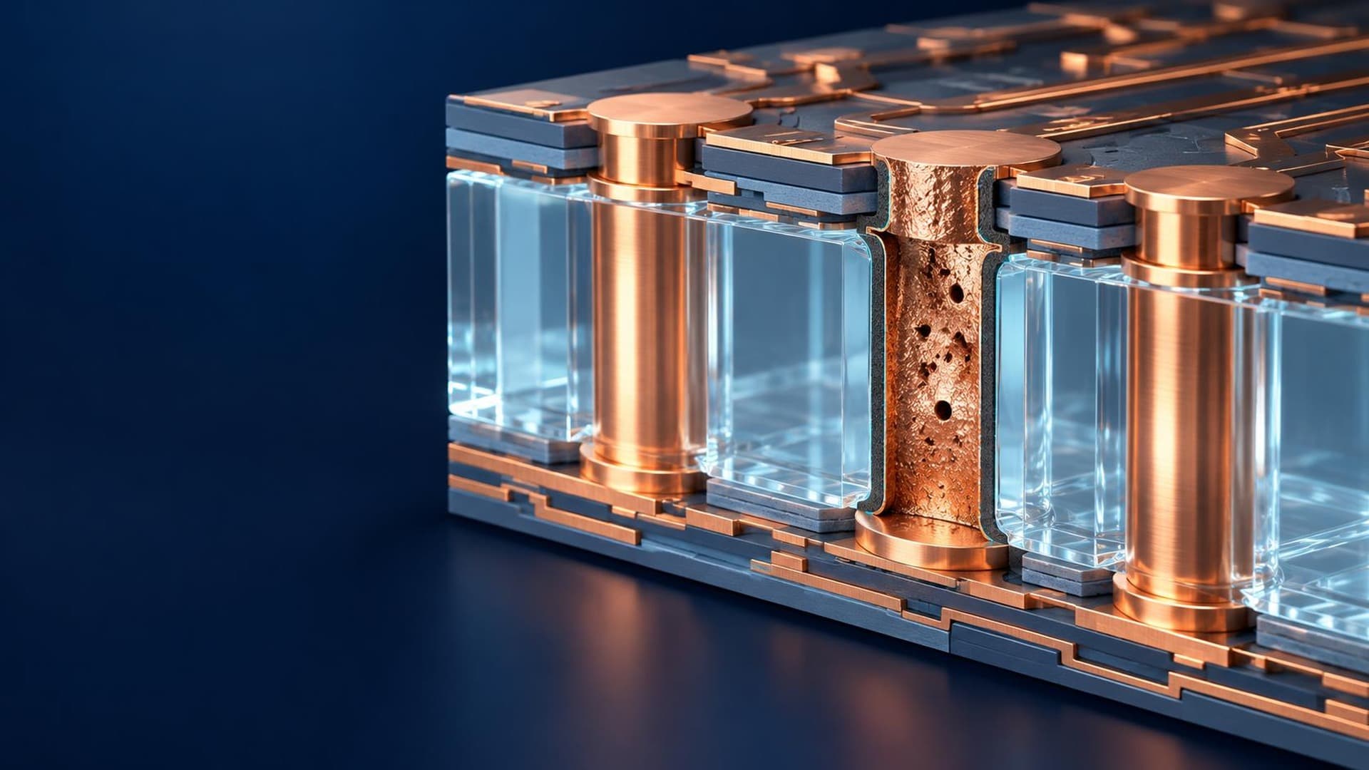
A metal-oxide adhesion layer secures adhesion between glass and copper, but hydrogen bubbles and nanovoids inside the electroless copper seed can form a separate failure path. Published work reports that voids in a 300 nm seed concentrate in the first 100 nm and grow larger at higher bath temperatures.
Conclusion
In through-glass via (TGV) metallization, a metal-oxide adhesion layer holds the copper to the glass. This document compares two commercial processes, Uyemura MOSL and Atotech VitroCoat, against published papers and patents, and divides what needs review into three layers: the oxide–glass interface, the oxide layer itself, and the interior and boundaries of the electroless copper seed on top. Its starting point is that the grain size on the oxide surface (20–50 nm) and the oxide film thickness are different quantities, and that even when adhesion is secured, the soundness of the copper seed must be checked on its own. For the seed interior the document draws on two papers. Nakahara (1988) observed small 2–30 nm bubbles throughout electroless copper films and bubbles of about 200 nm at grain boundaries, and explained the loss of ductility with a ductile fracture model based on void coalescence; a 150 °C post-anneal partly restores ductility lost to hydrogen pressure by releasing hydrogen. Hsieh et al. (2025) imaged voids by TEM in a 300 nm seed in a Cu/electroless Cu/Cu stack on FR4, finding that voids concentrate in the first 100 nm and that raising the bath temperature from 22 °C to 37 °C increased the void fraction in the initial lower layer from 1.3% to 6.1% and the maximum void size from 8.7 nm to 33.7 nm. The document notes that these specimens were not direct tests of TGV processes, and it labels the view of residual voids as crack initiation sites under thermal and mechanical load as an engineering interpretation. For the oxide interface and fine-via coating, it reads a patent and a 2015 conference paper together. A later patent states that copper can migrate through the oxide layer to the glass surface during post-annealing and weaken adhesion, and describes adding Ni or similar elements to the copper film along with the resistivity and plating-uniformity costs this brings. The 2015 paper reports blockage rates that varied with pitch for the same via shape together with blockage-free results for larger vias; the document limits these to the experiments of that time. Its conclusion is that a production decision needs both adhesion and seed soundness. Electrical continuity, initial peel strength and long-term mechanical reliability are separate criteria, and the document states that this evidence alone cannot establish whether any specific supplier can reach volume production, nor that all electroless copper must fail.
References
- 1. Nakahara, S. (1988). Microscopic mechanism of the hydrogen effect on the ductility of electroless copper. Acta Metallurgica, 36(7), 1669–1681. https://doi.org/10.1016/0001-6160(88)90234-9
- 2. Hsieh, M., Zhang, Z., Nishijima, M., Okumura, R., Seto, H., Nishikawa, H., & Suganuma, K. (2025). Mechanism of void growth in electroless copper plating layer of microvias in high-density interconnect packaging substrates. Journal of Materials Science: Materials in Engineering, 21(1), 5. https://doi.org/10.1186/s40712-025-00374-w
- 3. Liu et al. (2015). IMAPS 2015 학회 발표 논문(VitroCoat 공정).
- 4. US20260226629A1 (우에무라 출원 특허).
Topics
- Glass substrates
- Plating