About this document
This Technical Note describes printing a PDA pattern on the substrate first so that only the places that need circuitry become adhesion and metallization areas. It sets out the two metallization routes, electroless plating and paste printing, that branch from the same PDA pattern.
Download
An English edition is not available yet. The Korean document is below.
Summary
With a PDA pattern printed first, the PDA at the interface handles adhesion and the copper or silver line above it handles conduction. Electroless plating grows metal selectively on the PDA areas and suits fine lines; paste printing uses aligned printing and sintering and suits thicker conductors. The note covers a stack shared by glass and organic substrates and applications in sensors, heaters and antennas.
Conclusion
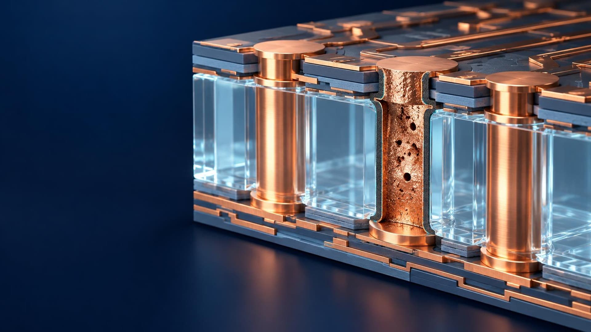
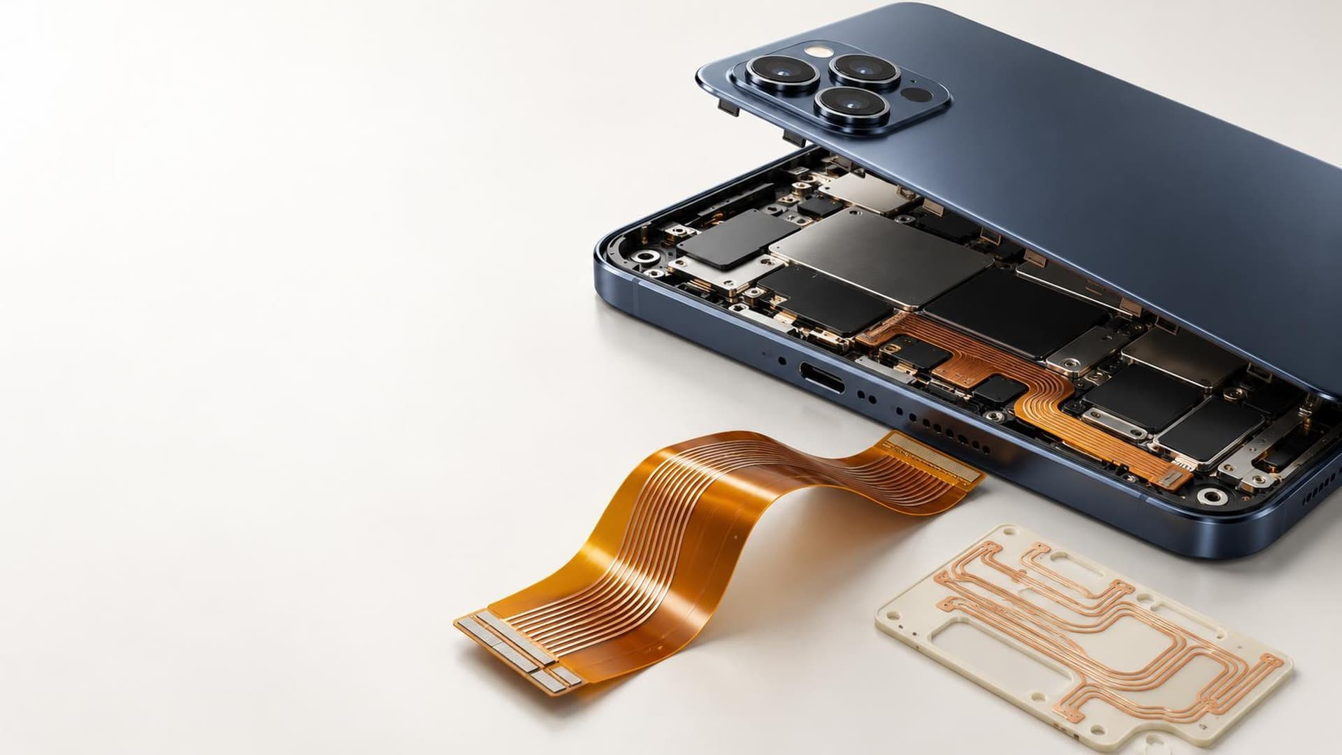
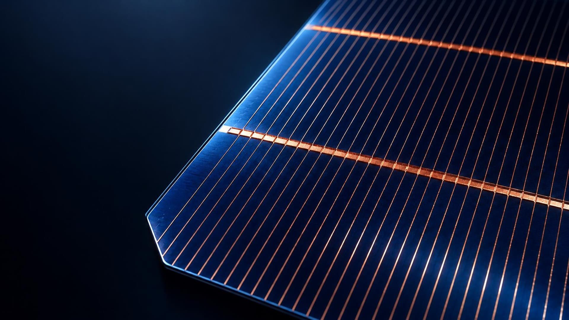
The stack has three layers: the substrate, a PDA adhesion interface and a Cu or Ag metal line. Adhesion sits at the interface and conduction in the metal line. Glass and organic substrates use the same structure, with only temperature, solvent and surface preparation adjusted per substrate. The process starts with surface preparation, PDA pattern printing, and drying and fixing. PDA is printed in the designed circuit geometry with line width, spacing and print volume controlled so that the lines stay continuous. The quality of this PDA pattern governs where the subsequent metal lines sit and whether they stay continuous. Metallization then branches. Electroless plating nucleates metal on the PDA areas and grows it selectively in place, with thickness set by plating conditions and time; it is used for fine lines and complex circuit patterns. Paste printing aligns Cu or Ag paste onto the PDA areas and connects it by drying and sintering, with thickness set by deposition volume, number of passes and sintering; it is used for thicker conductors and integration with existing printing lines. On that route, final line width depends on the precision of both the PDA pattern and the paste print. With copper, a thin PDA treatment on the particle surface suppresses oxidation, interparticle connection forms the current path, and PDA at the bottom bonds the line to the substrate. The aim is to replace silver with copper while securing both adhesion and low line resistance. Changing circuit geometry and substrate extends the approach to transparent sensors and electrodes, where fine lines preserve optical aperture, flexible heaters on curved film, and antennas and interconnects that depend less on silver. The document presents this as a technical proposal ahead of confirmed performance and manufacturability, with PDA patterning ink, metal materials and substrate-specific processes as the supply concept.
Topics
- Printed electronics