About this document
This Technical Note addresses how roughening for adhesion raises high-frequency conductor loss on the low-loss PTFE and LCP substrates used for smartphone RF feed lines and antennas. It describes smooth metallization that bonds copper through a PDA interface instead of roughening.
Download
An English edition is not available yet. The Korean document is below.
Summary
A low-loss substrate does not remove conductor loss in the copper line, and roughening the substrate for adhesion also roughens the underside of the copper where current flows. A thin, continuous PDA layer bonds copper to the substrate while keeping the interface smooth, and circuits are built on an electroless copper seed with existing lithography and plating steps.
Conclusion
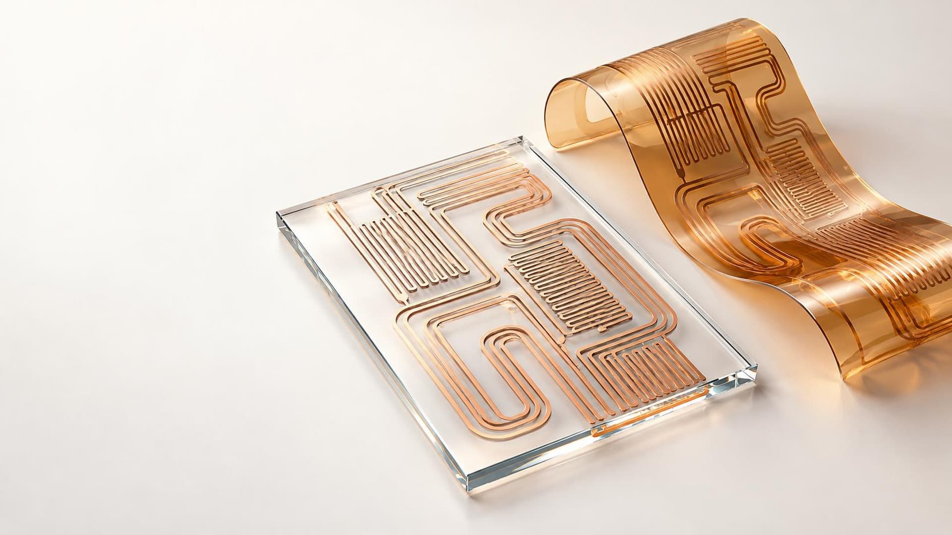
On the thin, long feed line between a smartphone RF module and its antenna, loss has two parts. Dielectric loss can be cut with low-loss substrates such as PTFE and LCP, but conductor loss in the copper line remains and depends on copper conductivity and interface roughness. The document focuses on adhesion and smoothness at the copper interface on low-loss substrates. The two requirements conflict. Roughening the substrate lets metal grip mechanically, but it also roughens the underside of the copper where high-frequency current flows. As frequency rises the conducting surface region thins: the skin depth of room-temperature bulk copper is 0.85 μm at 6 GHz and about 0.39 μm at 28 GHz (calculated). Roughness therefore has to be controlled on the substrate-facing underside of the copper as well as on its top. The Cools design obtains adhesion without roughening. Cleaning of the smooth surface, thin PDA treatment, activation and electroless copper seed growth form a continuous seed, which then joins the existing lithography and plating path of PR patterning, electroplating, PR strip and exposed-seed removal. The PR pattern sets the circuit geometry. PTFE and LCP share the same stacking principle with film formation adjusted to each substrate: uniform PDA formation and adhesion design on fluoropolymer surfaces, and smooth metallization linked to bending and lamination on thin LCP film. The document notes that identical process conditions do not imply identical adhesion. The document illustrates the benefit with a worked example. At 100 mW input, reducing line loss from 2 dB to 1 dB raises the power delivered to the antenna from 63.1 mW to 79.4 mW, an increase of 25.9%. This is not a Cools measurement; at constant delivered power it translates into room to lower input power. Application is to extend from LCP feed lines and antennas to PTFE RF substrates.
Topics
- Printed electronics