About this document
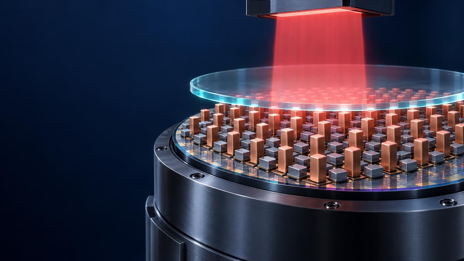
This Technical Note examines the burden that sputtered seed layers place on large-area RDL built on panels, as in CoPoS. It describes a wet metallization approach that changes only the seed-forming module, using a PDA interface layer and electroless copper.
Download
An English edition is not available yet. The Korean document is below.
Summary
At panel scale, sputter tools grow larger, and seed uniformity across the panel, compatibility with organic films and coverage of fine openings all become harder. Forming a continuous PDA film on a flat dielectric surface and then an electroless copper seed through catalyst loading turns the vacuum seed step into a wet one. The note covers SAP and embedded wiring flows that keep lithography, electroplating and seed etching unchanged.
Conclusion
The manufacturing base for the large-area RDL that CoPoS (chip-on-panel-on-substrate) needs already exists. TSMC has produced RDL interposers for CoWoS-R since 2023, and TOPPAN has developed damascene-based organic RDL and is extending it to large interposers through panel manufacturing. Lithography, dielectric lamination, pattern plating and line separation can be handled with existing capability. Where Cools comes in is the adhesion layer and Cu seed across the panel. Panel-size sputtering stacks up several burdens: larger chambers, targets and vacuum transfer, center-to-edge seed variation, outgassing and thermal history of organic films, and continuous seed coverage on the sidewalls and bottoms of fine openings. Interface flatness also matters for fine RDL. Roughening the base surface for adhesion leaves seed in the valleys, creating leakage paths between lines, and the roughness widens line-width and cross-section variation and lengthens the conductor surface path. On a flat interface, seed etching ends as a planar removal, which makes line-to-line isolation easier. Cools' PDA wet metallization proceeds through surface cleaning and preparation of the dielectric, formation of a continuous PDA film by aqueous surface polymerization, rinsing and film stabilization, loading of a Pd catalyst or metal ions, activation and reduction, and an electroless Cu seed followed by electrolytic Cu. In the RDL flow, only the seed-forming module changes; via formation, resist patterning, electrolytic Cu and stripping and seed etching use existing processes in the same positions. Two wiring structures follow. In SAP wiring, a plating resist is patterned over PDA and a blanket electroless seed on the dielectric, electrolytic Cu is grown in the openings, and the resist and exposed seed are removed to separate the lines; removing only the thin seed avoids the undercut and line-width loss of blanket etching thick Cu. In embedded RDL, trenches and vias are formed in a photosensitive organic dielectric, PDA is coated with the lower Cu pad contacts left open, the features are overfilled with electroless seed and electrolytic Cu, and CMP removes Cu, seed and PDA from the field to leave the wiring in the trenches. With the vacuum seed step no longer repeated for every layer, scaling up panel size becomes a matter of coating, baths and solution management, and existing plating lines can be used.
Topics
- Plating
- Packaging