About this document
This Technical Note describes how a functionalized silsesquioxane (SQ) coating can serve as the interface for forming copper in glass vias, RDL layers and on ABF substrates, and which process module changes in each application. The full report is available in Korean. An English summary is provided on this page.
Download
An English edition is not available yet. The Korean document is below.
Summary
Seeds in glass vias and RDL layers rely on vacuum sputtering, and copper adhesion on ABF relies on surface roughening. A functionalized SQ coating that is chemically anchored to the substrate captures catalysts or copper ions, forming a wet-processed seed and a smooth adhesion interface. The note covers the material design principles, the process change in each of the three applications, results from prior research and the first experimental setup.
Conclusion
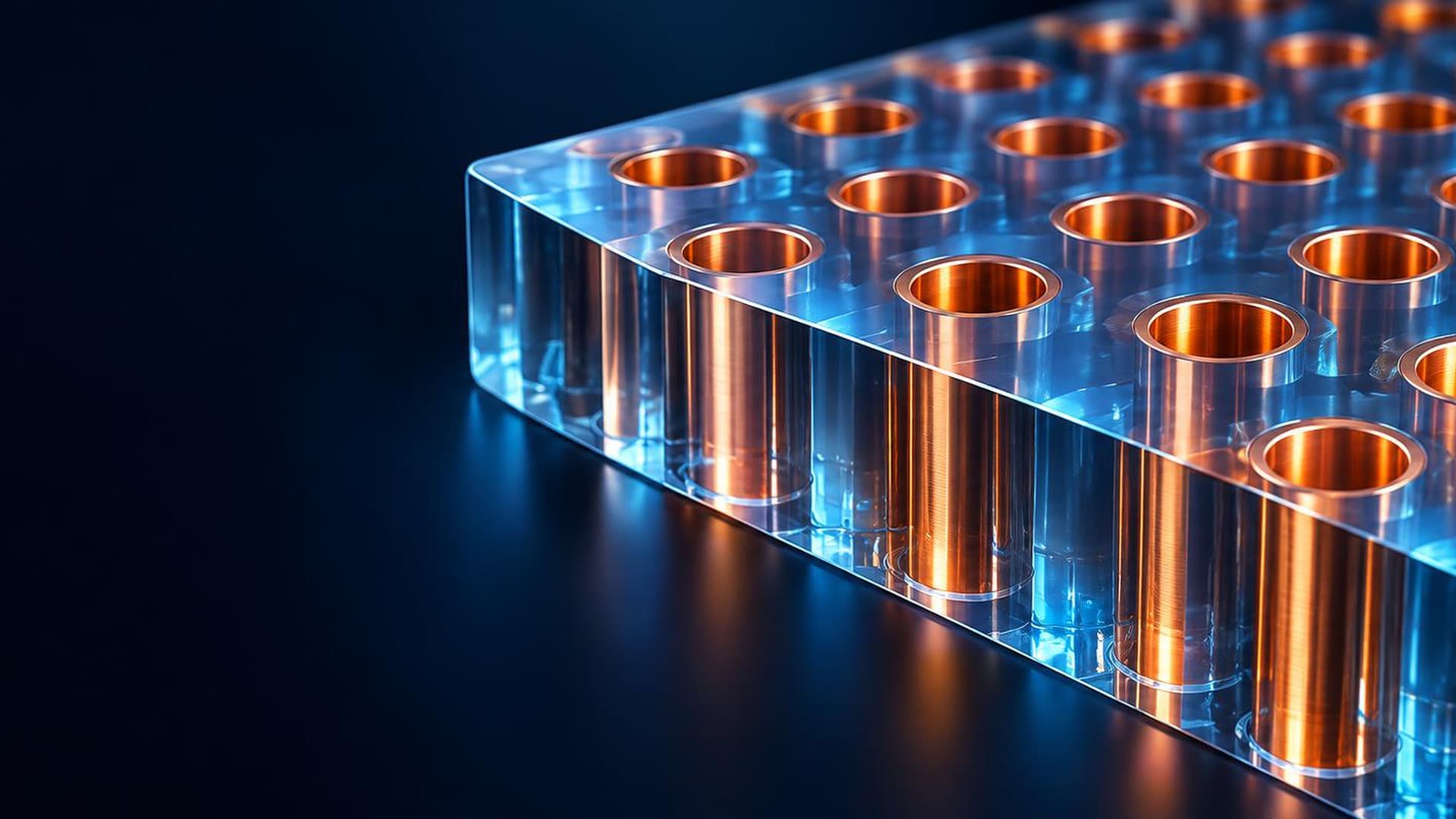
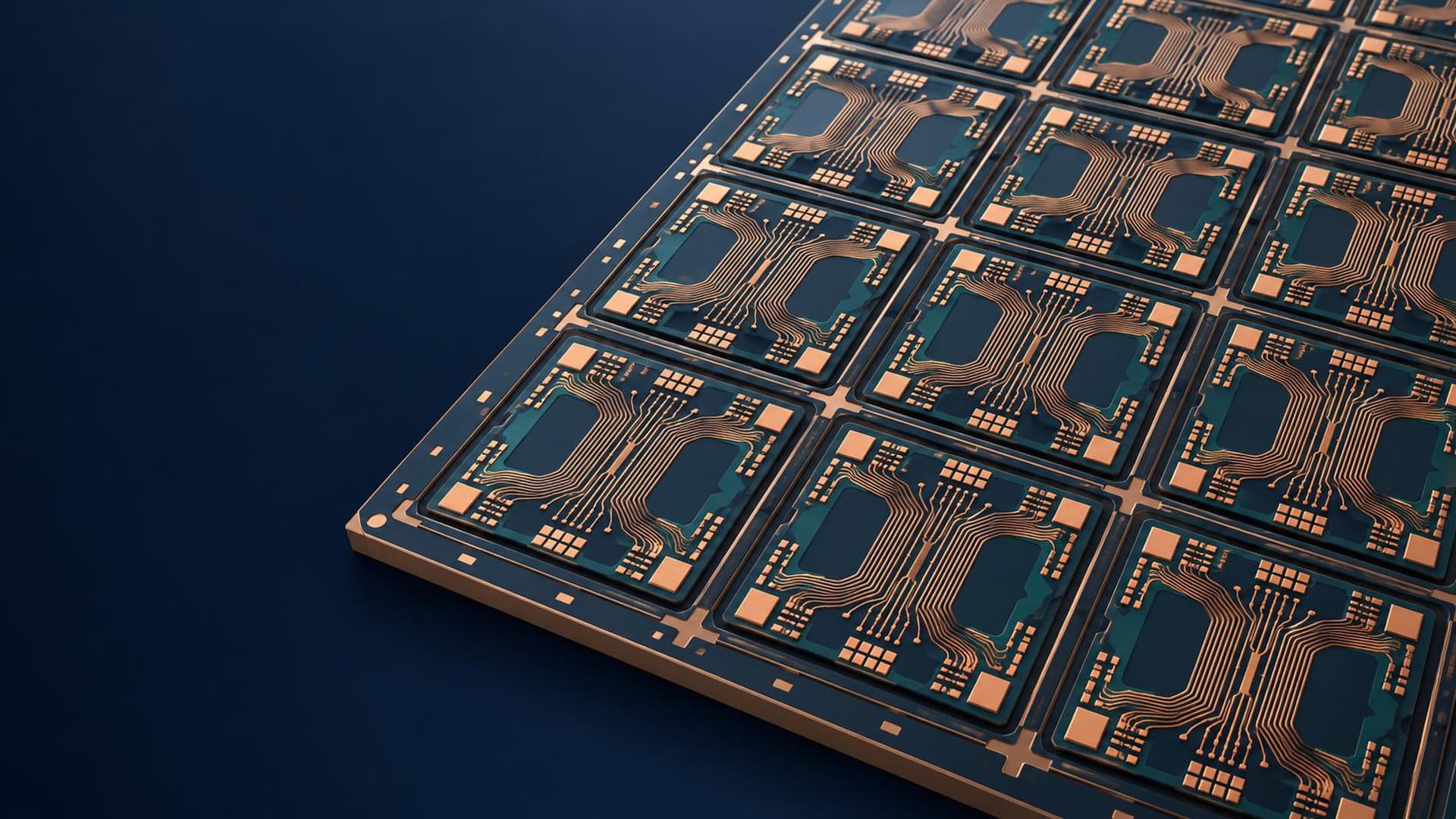
Glass vias, RDL layers and ABF substrates differ in shape but share the same problem: how to attach copper to an insulator and how to build the seed. The approach proposed here anchors a functionalized SQ coating to the substrate first and starts copper formation on top of it. Only the seed and interface formation module changes; lithography, copper electroplating and seed etching stay on the existing line. The functionalized SQ layer has three elements designed separately: a functional group that bonds to the substrate, a functional group that captures metal ions or catalysts, and curing conditions that fix the cross-linked network. Bond strength and film durability are not set by the backbone type alone, and both cage-type POSS and ladder-type PSQ are candidates. Functional groups are chosen by what they need to capture and which process they connect to, with no universal ranking among them. Any route that loads metal ions must include an activation and reduction step. In prior research (literature values), electroless copper lines were formed on polyimide (PI) coated with a functional PSQ at mask widths of 6, 5 and 4 μm, with resistivity of 3.8 to 7 μΩ·cm. At 2 μm no dense conductive path formed and resistivity rose to 66 μΩ·cm. In the same study, the SQ coating reduced the PI surface roughness Ra from 2.43 nm to 0.43 nm, about 82% lower. The original work defined line positions photochemically, whereas the process proposed here coats the whole surface and then uses existing lithography, electroplating and etching. For high-aspect-ratio TGVs, where line-of-sight deposition piles up at the entrance and on flat surfaces and thins out at the via center, a dip-coated wet seed is proposed. Wetting, trapped bubbles and drainage then determine coating continuity. A continuous electroless seed becomes the current path for electroplating, and electroplating conditions select a hollow or a filled via. A self-propagating electrode architecture (SPEA) route, in which deposition starts from a partial sputtered electrode only at the entrance and surface and the grown copper front becomes the cathode for the next deposition, is presented as a development path proposed by Cools. For RDL, the note separates SAP wiring that replaces the sputtered seed with an SQ wet seed from damascene-type wiring that uses the photosensitive dielectric as the mold and finishes with CMP. On ABF, permanganate desmear removes residue and roughens the surface at the same time. The proposed process keeps residue removal while suppressing the increase in roughness, and obtains adhesion through SQ interfacial bonding. Not creating new roughness and filling existing roughness are treated as distinct effects. A smooth interface leads to a thin, uniform seed and more process margin for fine lines; a possible reduction in conductor loss from copper interface roughness at high frequency is treated separately from the dielectric loss tangent. The first experiments screen on flat glass and then extend to TGVs and ABF, running reference samples (existing sputtered seed and roughened ABF) and control samples without SQ under the same conditions.
Topics
- Glass substrates
- Plating