About this document
In vias with aspect ratios of 10:1 and above, conventional sputtering leaves the seed broken on the deep sidewalls. This Technical Note describes a process that extends the sputtered seed at the via entrance down the PDA-coated wall by electrolytic growth.
Download
An English edition is not available yet. The Korean document is below.
Summary
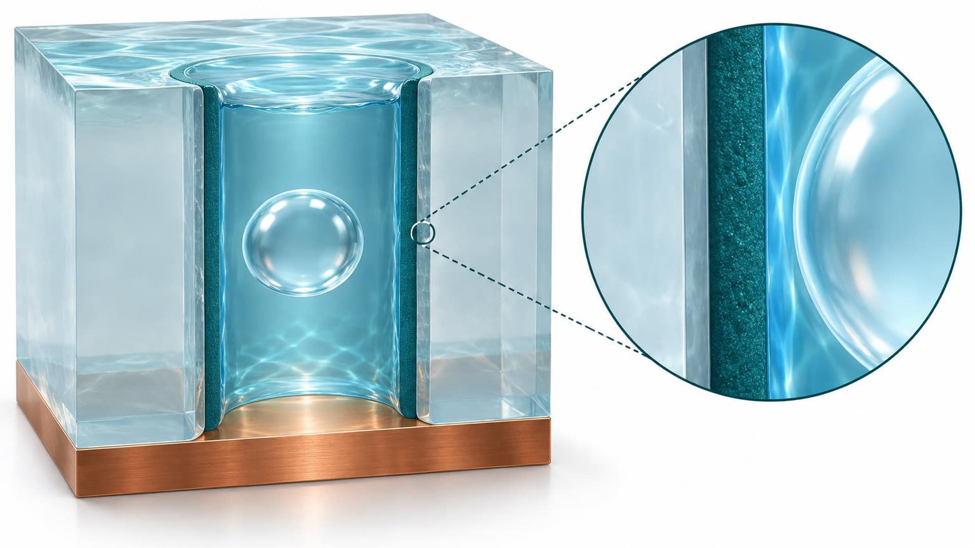
Sputtering deposits along the line of sight, so as vias get deeper the lower sidewalls are left uncovered and the current path breaks. A PDA interface is first formed on the via wall; the partial sputtered seed at the entrance then serves as the starting electrode, and metal grown at its edge becomes the next growth front, bridging the uncovered section.
Conclusion
Sputtering is a proven starting point for via plating: it forms a metal seed, supplies current from outside and leads into copper electroplating on established production lines. The document cites roughly 6:1 as the typical aspect-ratio range of conventional sputtering, noting that the actual range depends on via geometry, equipment and deposition conditions. Above 10:1 the limits of line-of-sight deposition grow. Deep sidewalls receive flux at low angles and are shadowed by the entrance, leaving uncovered regions that break the current path. The bottleneck is not film thickness but the continuity of a metal film running the full length of the via. The Cools process has three steps. A PDA interface is formed over the entire via wall so that metal can adhere deep inside. Partial sputtering with existing equipment then secures a seed near the entrance. Electroplating from that seed makes reduction and growth occur at the connected metal edge; each newly grown segment becomes the next growth front and advances into the uncovered region while staying bonded to the wall through the PDA interface. The point is to design edge growth and interfacial adhesion together. Two seed layouts are described. With single-sided sputtering, the seed edge advances from one entrance and connects the deep wall. With double-sided sputtering, the top and bottom seeds are fed at the same cathode potential and grow toward the uncovered middle. The goal of this step is to join the metal film at the center; filling the via is a separate plating step. The principle adapts the SPEA concept, in which grown metal becomes the next electrode, to sputtering, with the partial sputtered seed as the starting electrode and the PDA wall as the growth path. Once the seed is connected, conventional plating builds the target thickness and fill, extending the usable aspect-ratio range while keeping existing sputtering assets in use.
Topics
- Plating
- Glass substrates